
None of the ready-made modules with multiple output voltages turned out to be ideal. They didn't have a current readout, or were way too big to build in a small module case. The wish list therefore led to a plan for DIY. The test set-up and first test program in the previous part were a good proof-of-concept of current measurement with the INA3221 I2C current sensor.
Now it's time to put everything together. So: designing and printing printed circuit boards and a 3D housing. Then? Assemble and test everything, of course. The movie gives a good picture of the assembly and how the module finally becomes a 'real' usable product.
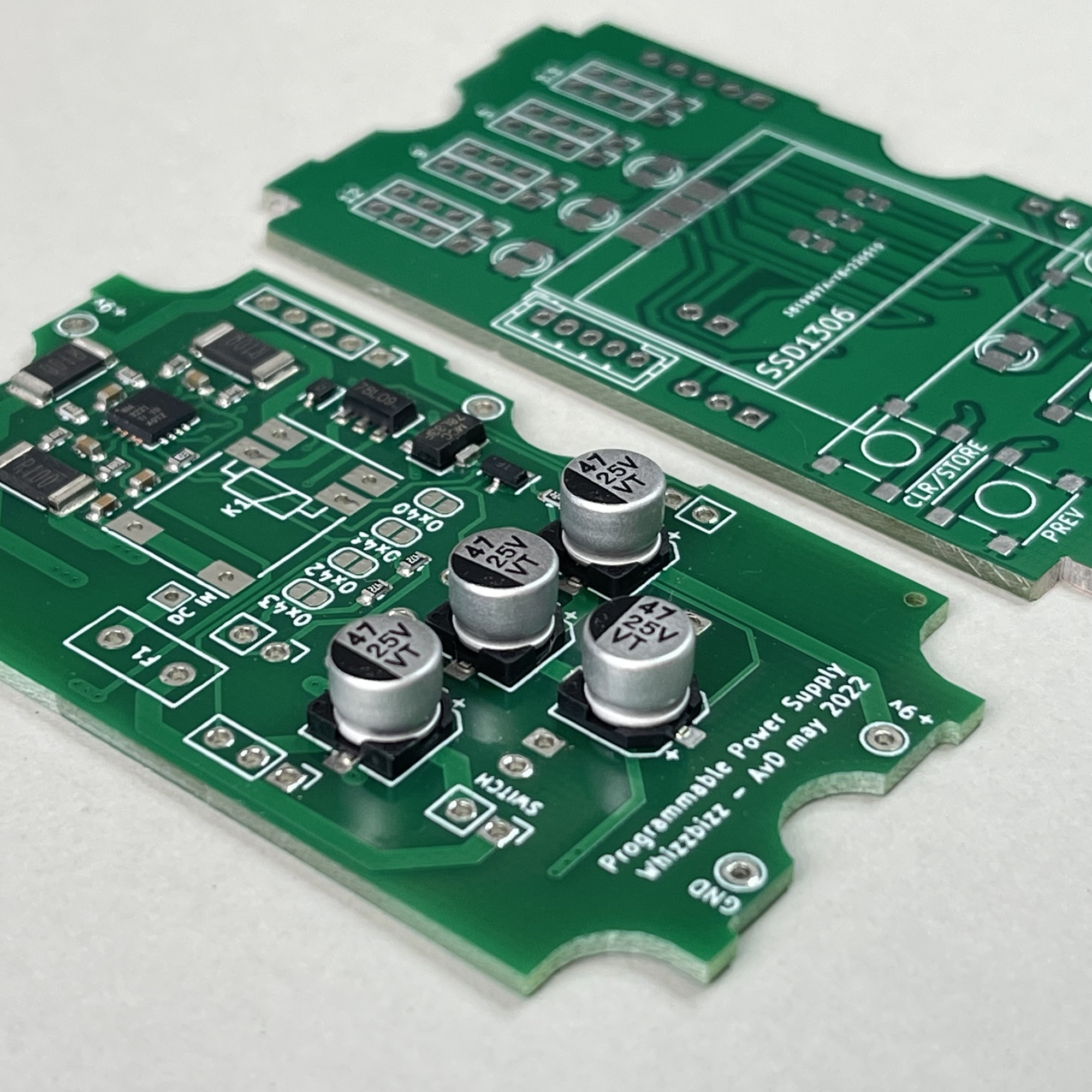
Because it would be nice if the final module could also be used as a power supply for the traditional fischertechnik 'Silberlingen' and the 'Zauberling', one of the original wishes was that it could be housed in a Silberling housing. The installation space of such a cabinet is only 3.5 by 7 centimeters with an installation depth of 2.5 cm. It was therefore clear from the start that, in order to make the most of this small space, the final module, like the Zauberling (photo opposite), would best be constructed from two stacked circuit boards.
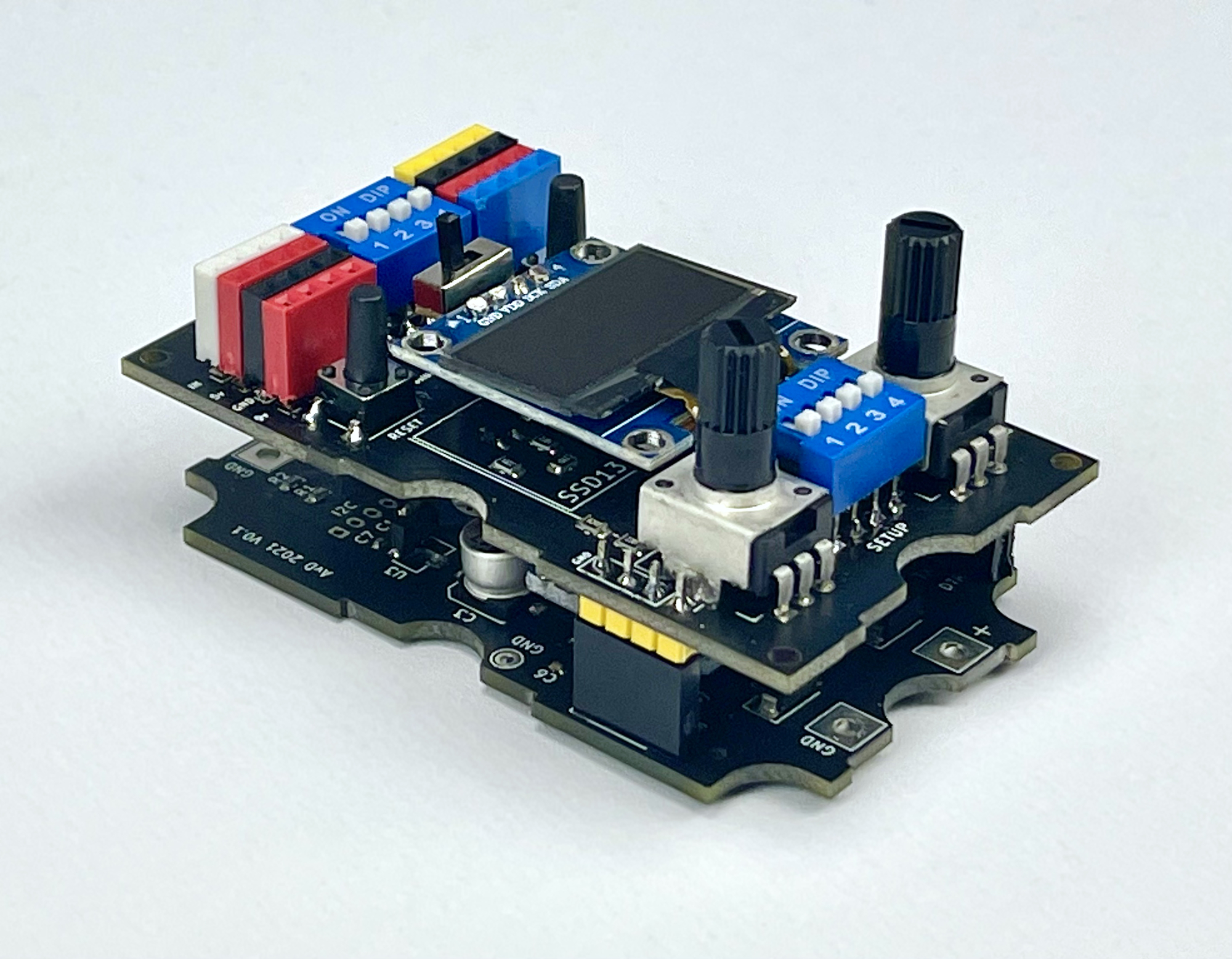
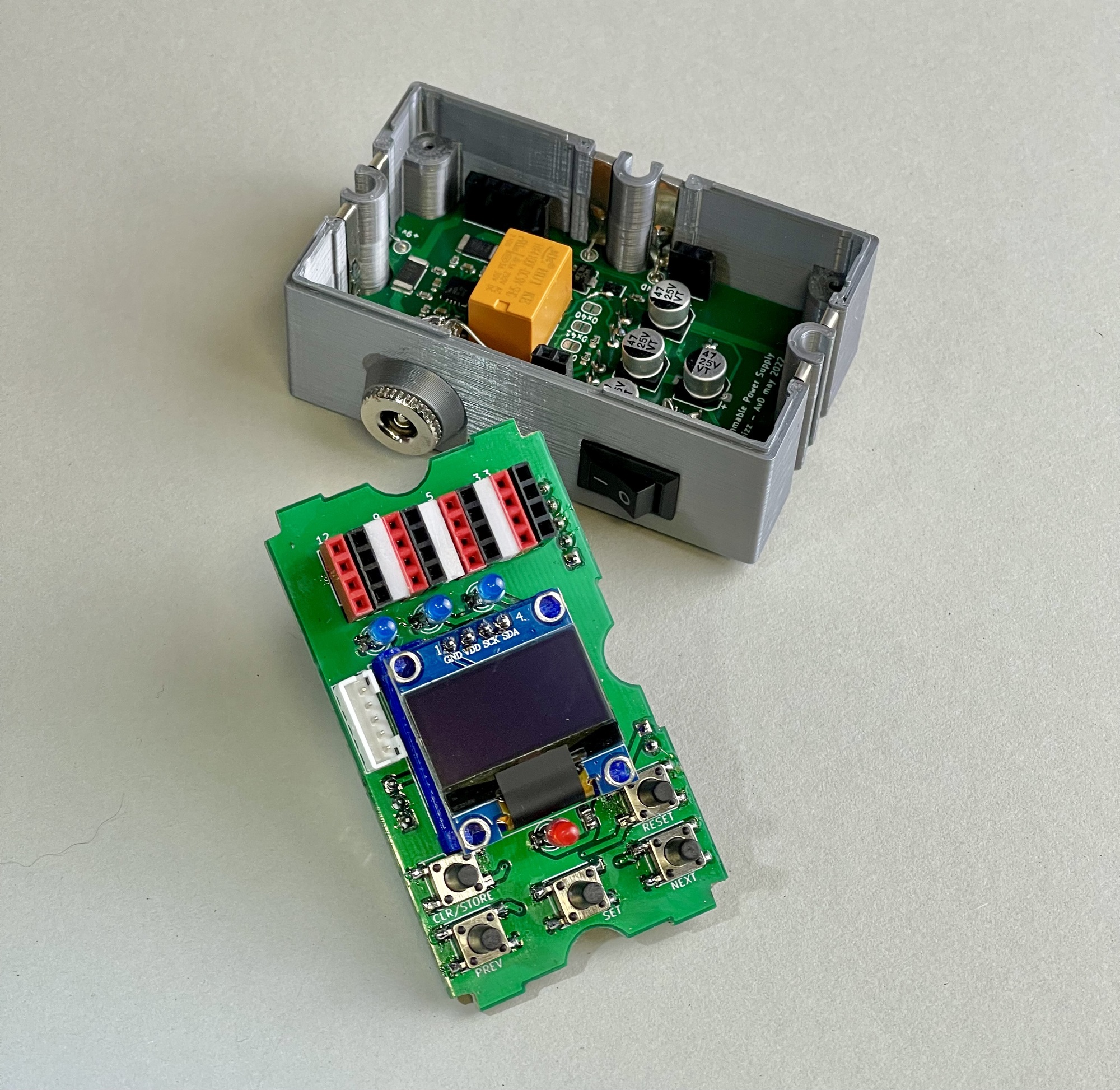
The gap between the PCBs is only 11mm and parts on the bottom of the upper PCB should not collide with tall parts on the lower PCB. In addition, a relay that is already higher than 11 mm must be accommodated on the printed circuit board to be designed now. Fortunately, the printed circuit board at the bottom of the housing could drop slightly, so that the front plate with all LEDs, connectors, push buttons and the display could remain at the same height as with the Zauberling.
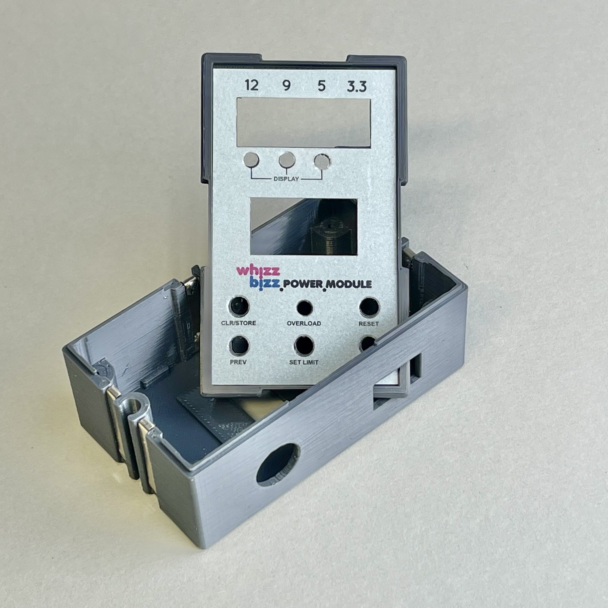
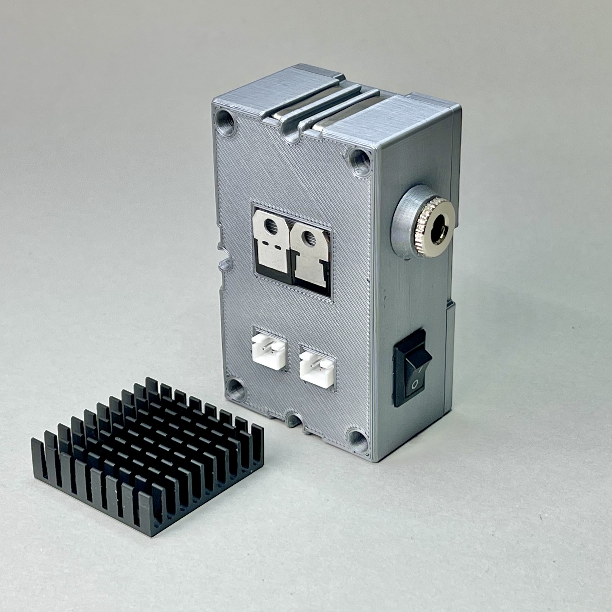
Connecting an external power supply to the rear of the module is optional with the Zauberling. With a 'power module' like this it would be nicer to be able to connect a 12 volt DC adapter directly. The module should also preferably have an easily accessible on/off button. Because in practice the position of this power supply module will always be on the far left in a row of 'Silberlings', the left side of the module can be used for this. However, when designing the printed circuit boards, it should be taken into account that the DC plug and switch protrude quite far into the housing.
Both components should fall pretty precisely between the two circuit boards inside the case. With an increase ring for the DC plug, we could save a few millimeters of installation space inside the cabinet. Yes, it's a tight fit!
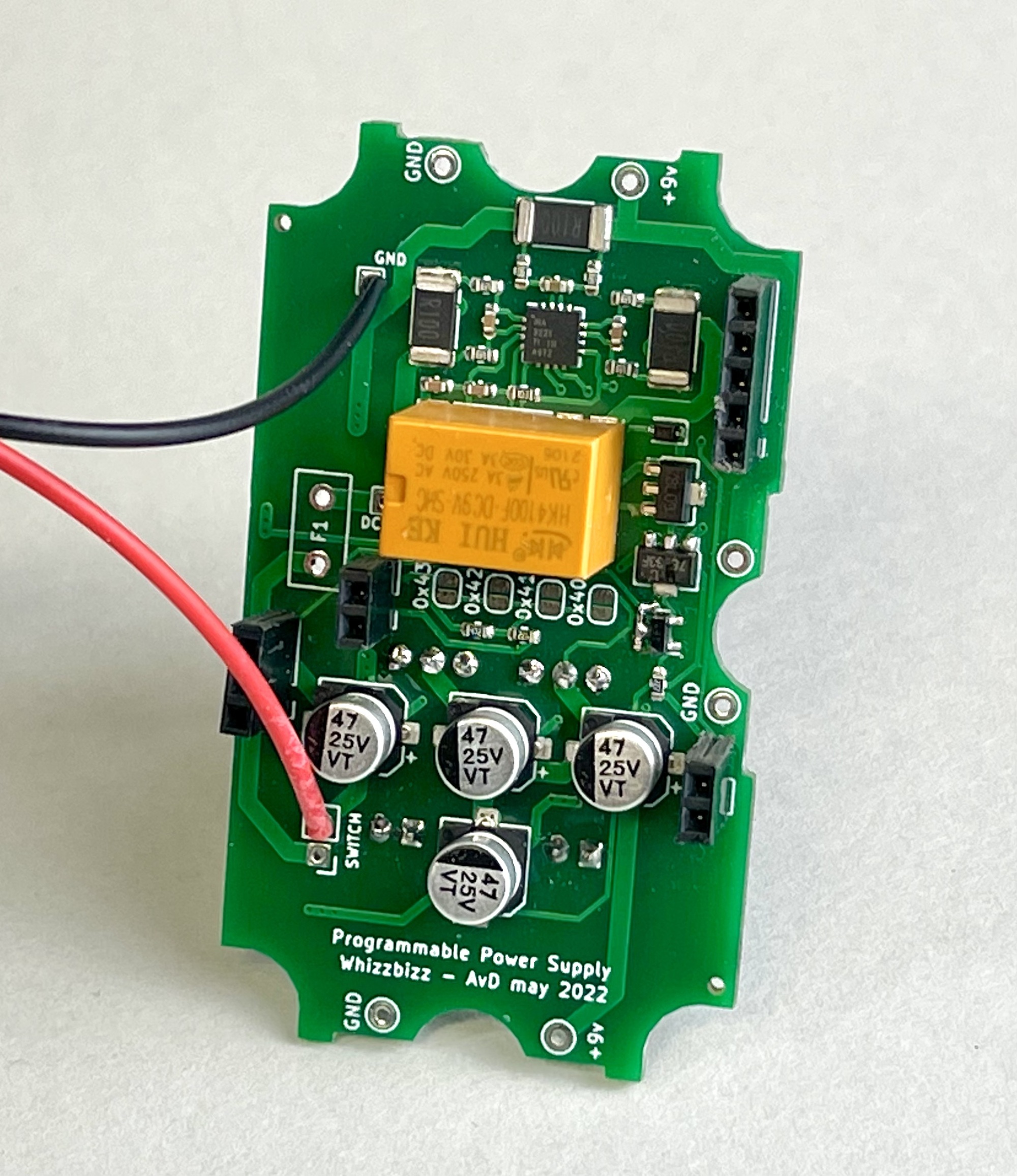
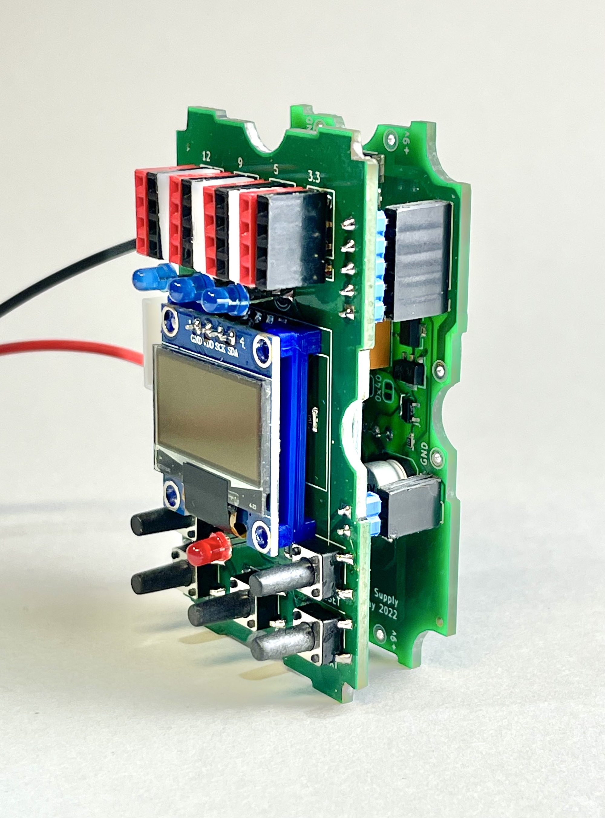
For the lower currents, such as with the 3.3 and the 9 system voltages, small 100 mA voltage regulators in SMD technology are sufficient. But for the 5 and 9 volts heavier voltage regulators are needed. When loaded, these could even become (slightly) warm, so it would be nice if they could protrude outside the cabinet at the back.
The module's firmware will not change that often. This eliminates the need for an external I2C bus or easily accessible FTDI programming port on the back of the module. This frees up a part on the back of the box for an opening for the voltage regulators. If the back of the module were to remain completely flat, a self-adhesive cooling element could provide the possible cooling.
The space between the printed circuit boards is quite small and the relay relatively high. There is also a DC plug and switch that is to be partly inserted into the case. So, designing in KiCad was a painstaking job. To prevent disruptive influences around the sensor as much as possible, I followed the datasheet as much as possible for the placement of the parts around the INA chip. I also adopted the proposed RF filter on the bus inputs.
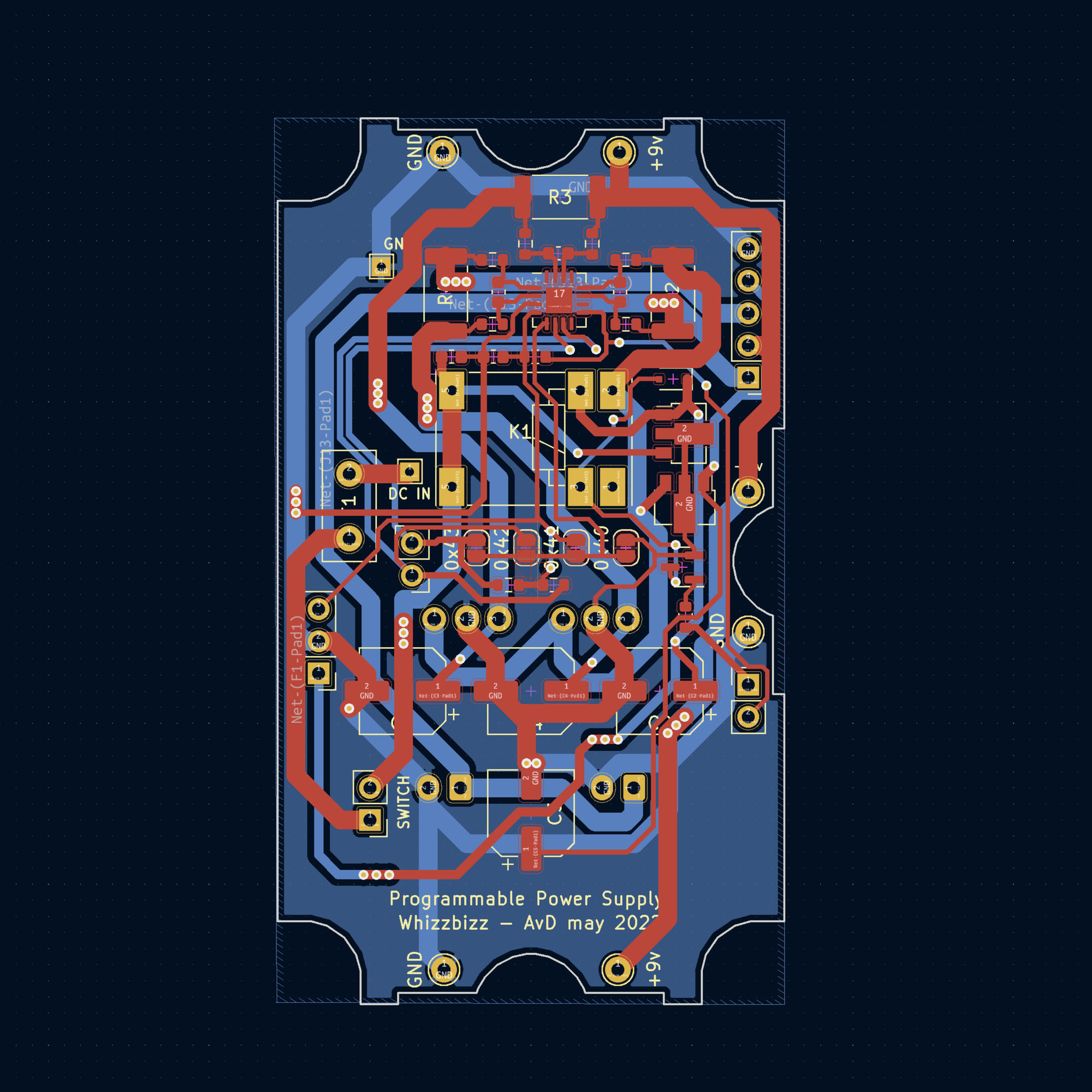
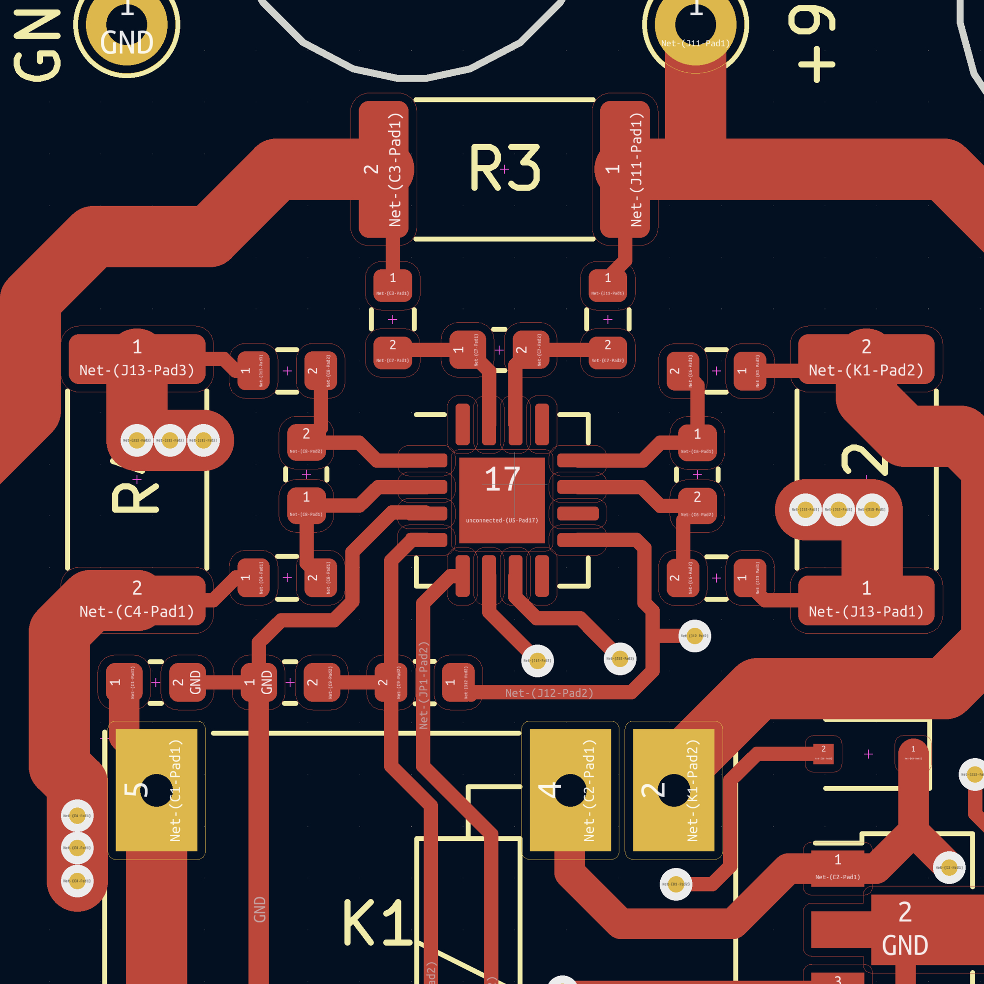
The track width of the tracks of the output voltages, which must be able to carry more current, has been kept as wide as possible. Online calculators and tables indicate that with the chosen track width of 1.5 mm, currents up to 1.6 Ampere should not cause any problems. I've simply opted for 1 ounce (oz/ft2) copper thickness for now, but this could be increased to 2 ounces. It is also possible to omit these traces from the solder mask so that they can still be manually tinned. Currents of 5 amps or more should then be possible, but none of this is necessary for my expected use. So I gave the module a physical fuse at the input of 1600 mA.
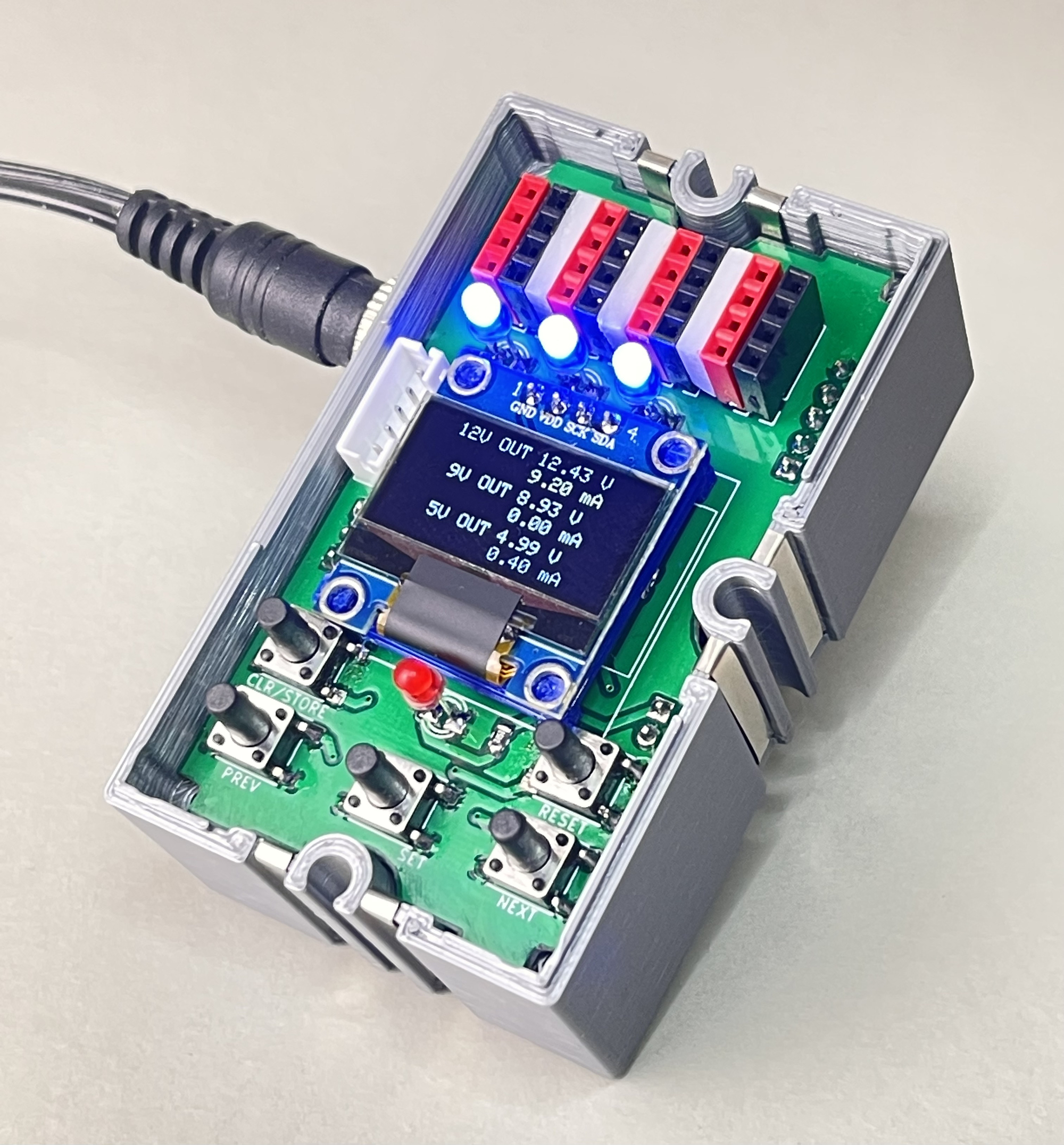
Pretty usable printed circuit boards could be made from the designs fairly quickly, which quickly yielded a testable result after manually adding the missing parts. The INA PCB was tested before installation with the Sketch, which could also be used for the test setup on the breadboard (see part 2).
On the printed circuit board on which the current measurements are performed, I had already had most of the SMD parts placed by the manufacturer. Although I have the soldering technique for it, I thought it was more than worth the extra cost. It saves a lot of time and especially placing the INA chip is a precision job. After the missing parts had been placed, the printed circuit board could be tested.
However, the 5 volt supply voltage for the INA chip is supplied in the final printed circuit board sandwich by the Arduino Pro Mini on the top circuit board, which is still missing. Fortunately, this could easily be solved by temporarily inserting a 5 volt voltage regulator (78L05) into the three-pin socket on the left. The test program from part 2 showed that the INA chip was indeed 'alive' and that its measured values could be delivered neatly over the I2C bus!
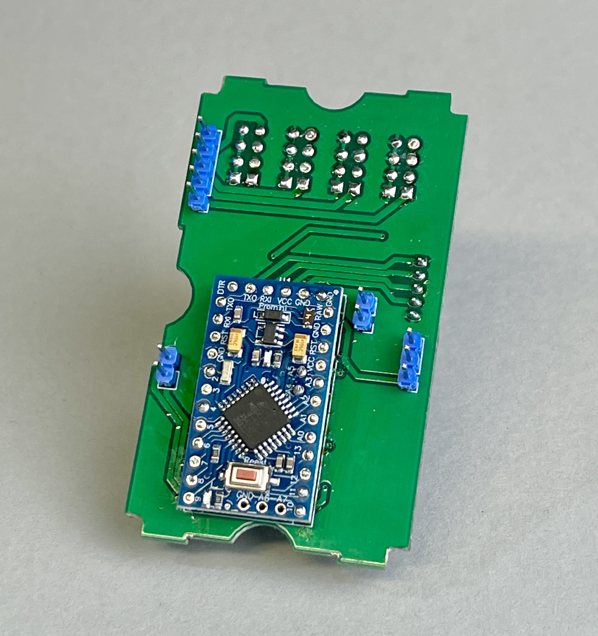
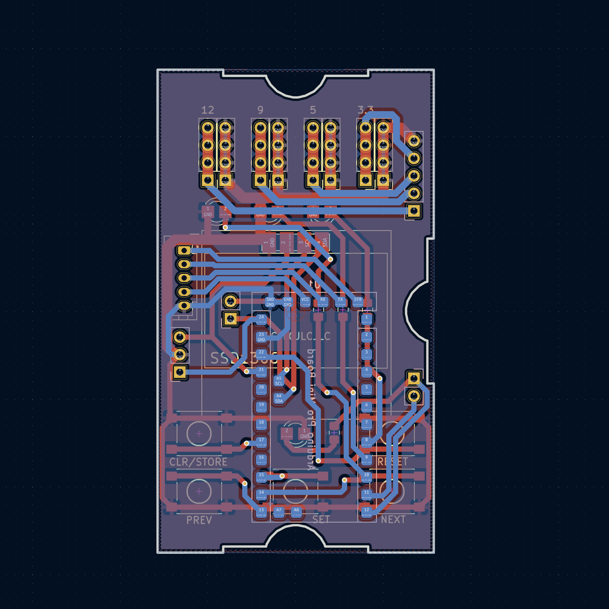
Most components of the upper circuit board were soldered on in a sort of semi-SMD-like technique. For example, the microprocessor hangs upside down like a kind of stilt house soldered to SMD copper islands. A technique that I also used with the Zauberling and which allows optimal use of all sides of the printed circuit boards.
This also makes optimal use of the space between the two printed circuit boards. During the component arrangement, however, it was necessary to be careful that nothing 'collides' with the high relay that dominates this space. Components that came out through the front and therefore prefer to be in a specific place, already occupy specific spots on the PCB. Other components just had to adapt. This explains the perhaps strange arrangement of the blue connection connectors.
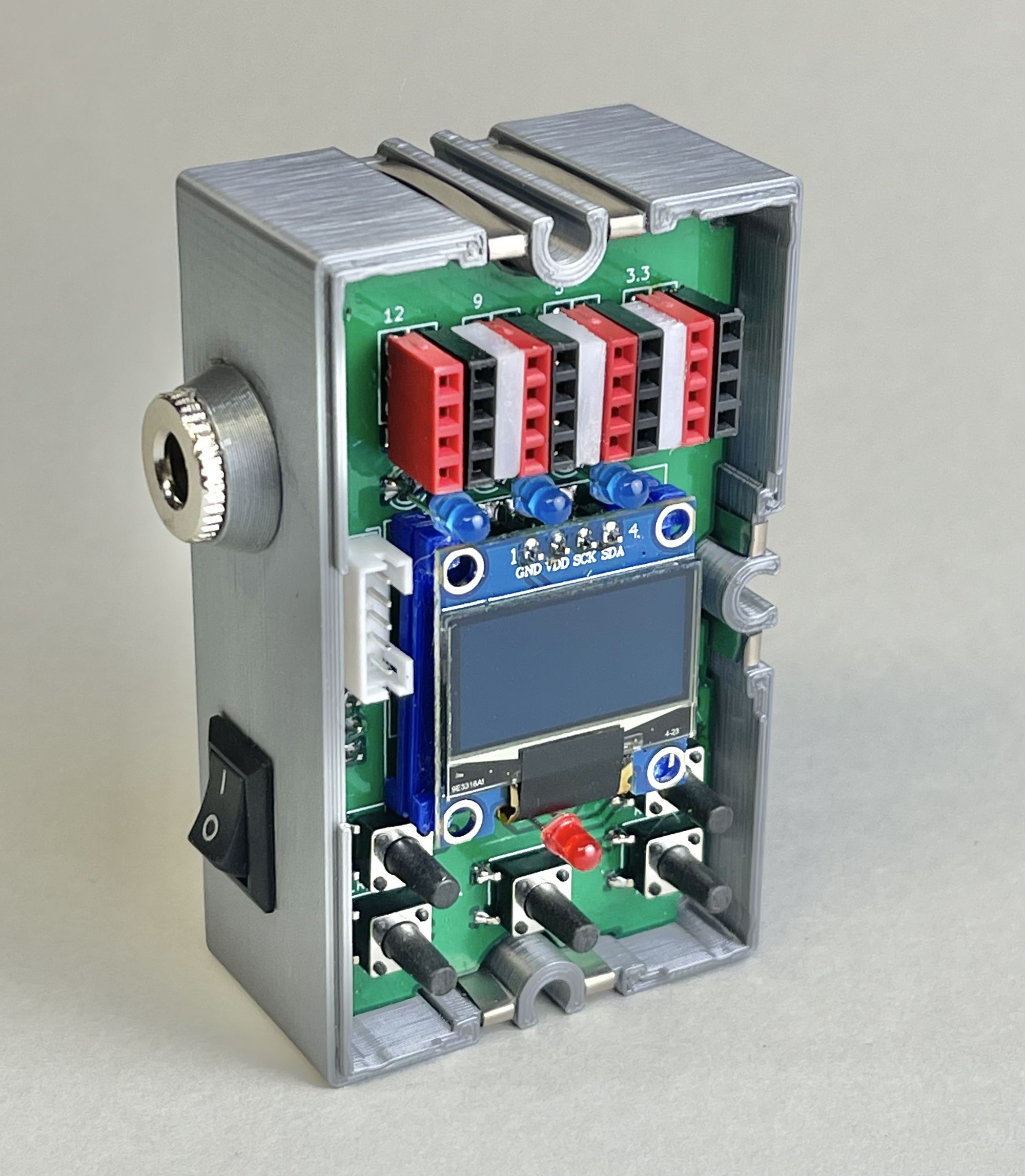
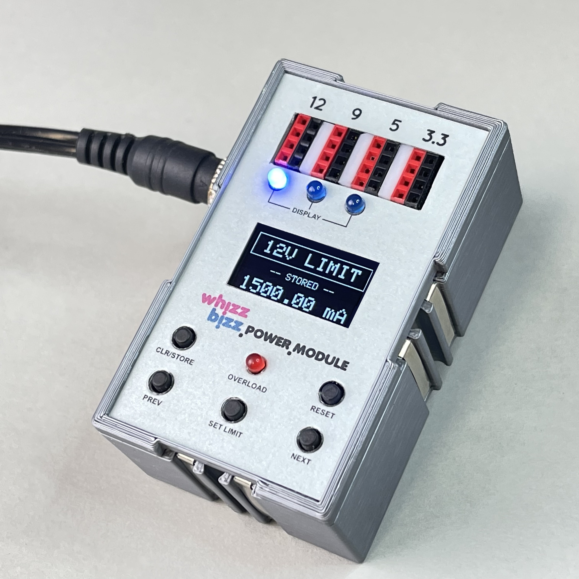
After assembling and programming the Arduino, the 'Ultimate Multi Power Module' was a fact. The readout and current limiting work fine. 3.3, 5, 9 and 12 volts are available on the front and the module can be easily combined with other modules.
I have put the latest version of the Sketch on Github. However, this software is likely still under development. When loaded with an inductive load, the measurement result on the display is a bit nervous, for this I will certainly want to experiment some more in the future with the configurable sampling frequency and the automatic averaging of the measured values by the INA3221 sensor.
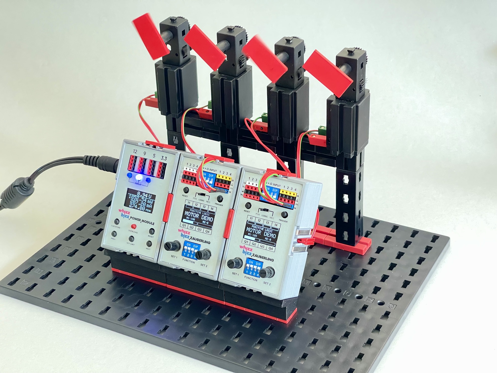
I conclude for now with a simple application example in the photo below. A four double 9 volt motor demo with two Zauberlings. Finally I have a clear view on the power consumption of fischertechnik motors. 😉
If you want to build the module exactly as I did, you can find the STL files of the case and the front design on Printables or Thingiverse where I have published them as 'Remix' of my original Silberlingen case variants.
The so-called Gerber files with the print design of both printed circuit boards turned out not to be completely perfect after production. There were 2 vias missing (which I had placed correctly?!) and I forgot the drill holes for mounting in the top PCB. Fortunately, with knowledge of the facts, this was easy to correct for me. However, I haven't bothered to correct this in KiCad yet. That's why I didn't think it is useful to publish these files yet. So design your own PCB, or feel free to ask me if you really can't figure it out.