
It was an instructive challenge to build the prototype of the magical Zauberling with Arduino Pro Mini in the relatively small internal dimensions of the original Silberling case (40 x 70 mm and only 25 mm deep). Editing the laser-engraved front plates by hand was also quite labour-intensive, but was ultimately successful.
The strength of the Zauberling lies in the collaboration with the traditional Silberlingen, but also with their own congeners. However, the prospect of going through this entire labour-intensive production process several times did not seem very attractive to me. In addition, there were naturally advancing insights, ideas for improvement and other additional wishes, so I soon started fantasizing about a version 0.2 with a more streamlined 'production process'.
A big improvement would be to design and produce neatly optimized printed circuit boards for the follow-up models. Because various online PCB production parties also offer an assembly service, space-saving SMD technology could also be used then. It seemed a very pleasant prospect to me that mainly assembly work was left for the 'series production' in this case.
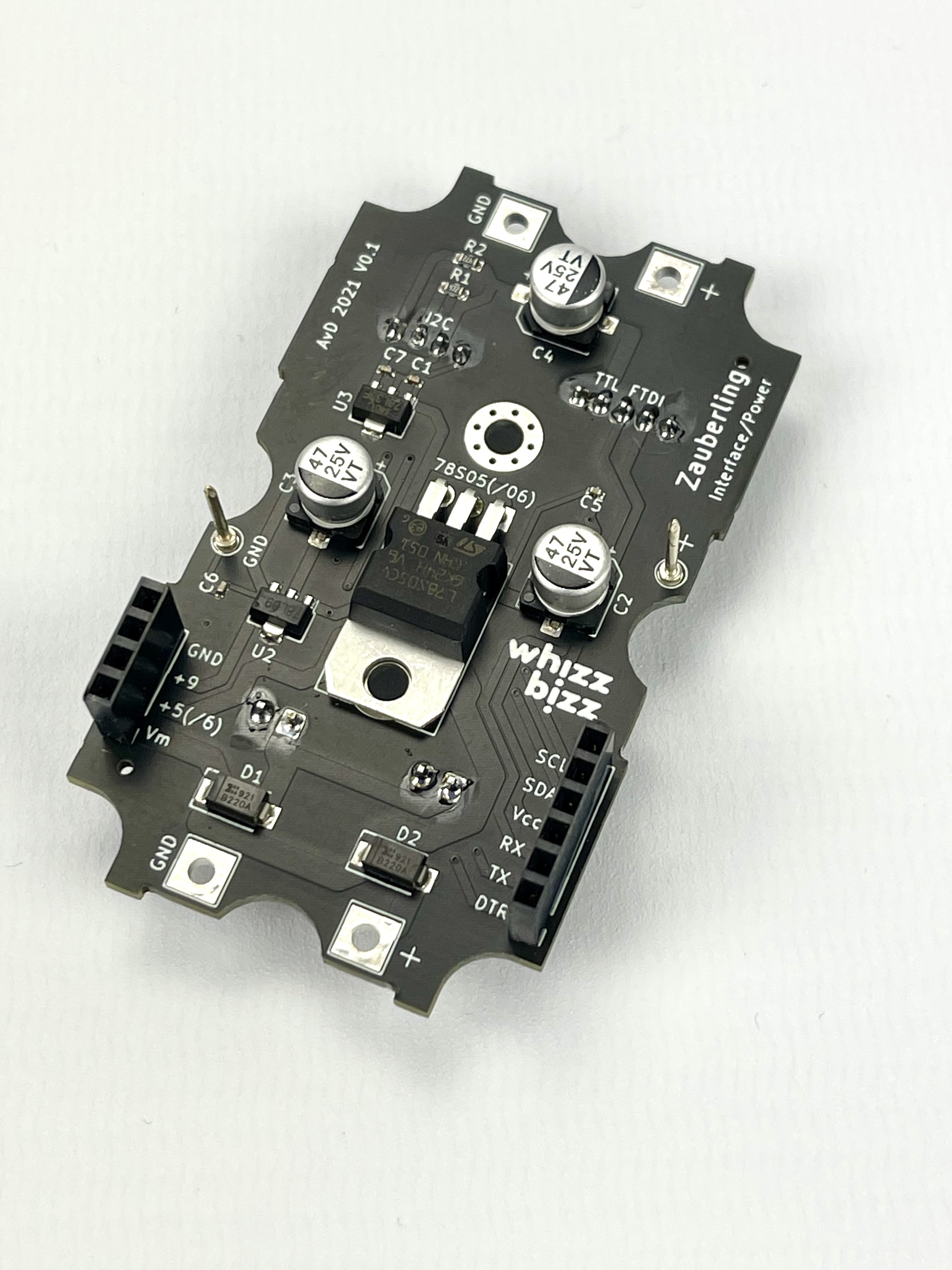
On the prototype of the Zauberling I had made the connections of the external power supply on the back with pieces of wire with connectors. The voltage regulators were mounted on the outside at the back for possible cooling, but mainly because I simply did not have room for them on the main PCB. This is sufficient for a prototype, but a logical next step is to design a more universal power supply board. In addition to the voltage regulators, the connectors on the back of the Zauberling could also be neatly located on such a PCB.
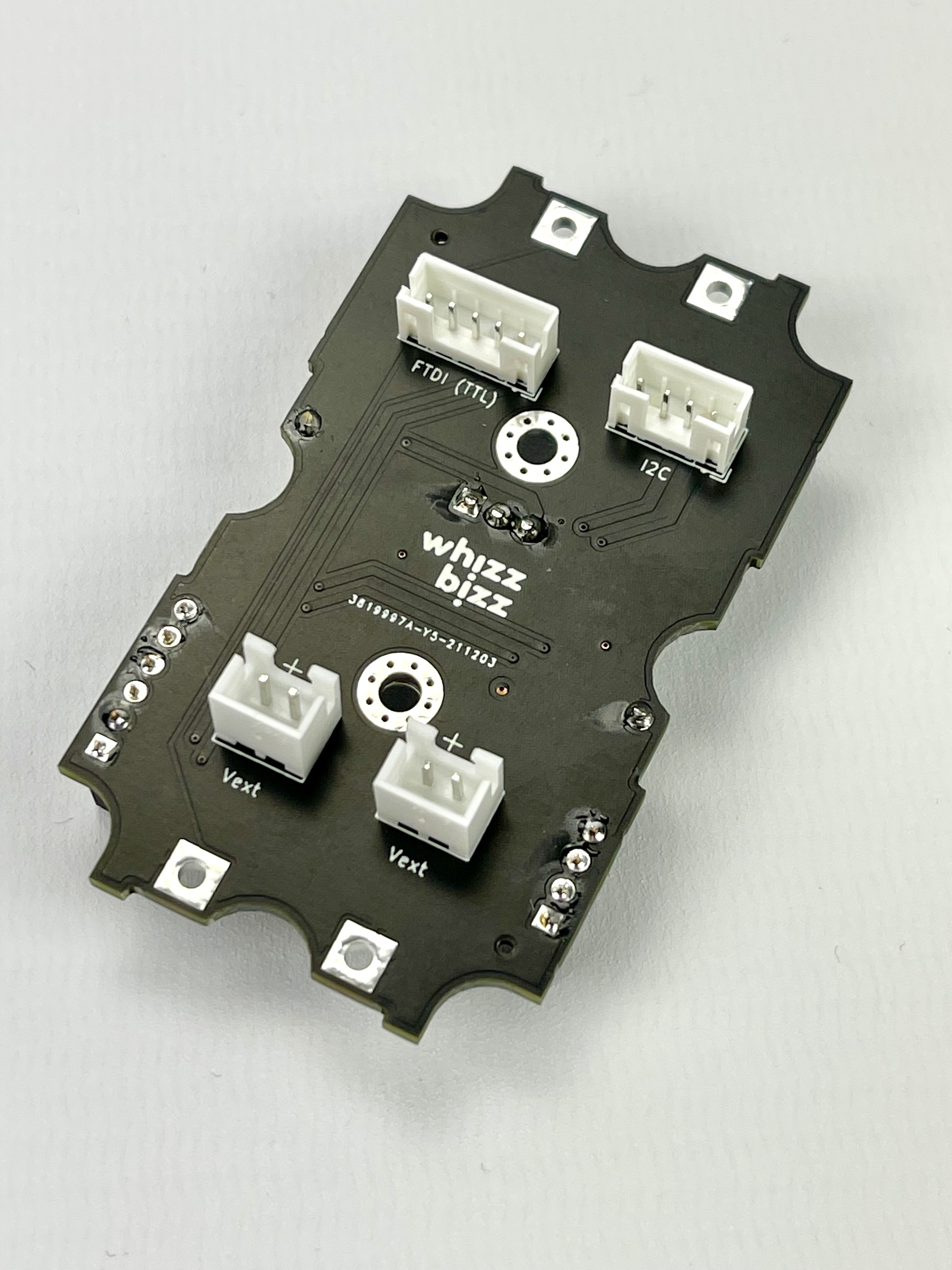
In any case, this would be an elegant solution for connecting, and possibly daisy-chaining, the optional external 12-volt power supply. For these connections 2-pin JST-HX connectors seemed suitable. These cannot be connected the wrong way round and the cables are relatively easy to make yourself.
On the Zauberling prototype, a small slide switch made it possible to choose between the regular 9 volts of the Silberling (provided via the sides with the connection clips) or the optional external power supply connected on the rear. If you don't want to run motors, the driver outputs don't need to deliver much power. In this case it is useful if the Zauberling could also be used without additional power supply. After all, the power consumption during purely 'digital' use, for example as a flip-flop, is quite limited. In many cases it would suffice to work directly from the power supply via the traditional fischertechnik rectifier module. Just as has been the case for decades with the original fischertechnik modules.
The automatic switchover to any external power supply and the facilitation of the various connections on the rear of the Zauberling could ideally be accommodated on a separate small PCB at the bottom of the case.
By designing a specific PCB for this, I could gain experience with today's design software and the current possibilities for online printed circuit board fabrication. Because it was already about 30 years ago that I made my own prints, I had not followed these developments for a long time.
The (TTL level) programming interface of the Arduino Pro Mini and the I2C bus for connecting external sensors could therefore be made available directly on such a universal PCB. The PCB would also be able to supply any required pull-up resistors and supply voltage (usually 3.3 or 5 volts) for the I2C bus. Because I wanted the freedom to choose a 3.3 volt I2C bus, if that would be necessary for certain sensors in the future, it seemed smart to implement the voltage supply of the I2C bus with a separate voltage regulator. An 'L' type (maximum 100mA) is more than sufficient for this. In addition, should this be useful in the future, a different voltage (eg 6 volts for a module that mainly drives servos) could be chosen for the large voltage regulator.
Male headers (print pins) are often chosen for the output of an I2C bus. This has the advantage that it is easy to work with ribbon cable. Because I expected that I would tailor the cables myself for each sensor or coupling, I eventually opted for SMH200/HY connectors. Due to their frame, these protrude a little neater through the back and still have the slight advantage of being compatible with Seeed's Grove sensors and breakout boards.
The PCB to be developed will serve as a connection option for the I2C bus and the TTL level programming interface. But mainly to provide the different supply voltages to the main PCB of the future Zauberling version, or whatever else I would like to install in a Silberling case in the future. Because it should not be mandatory to always connect an external power supply, it would be nice if, in addition to 5 volts (for the microcontroller) and 9 volts (to remain compatible with the Silberlingen logic), there would also be a pin available that automatically carries either the supplied power supply or the voltage from the side of the Zauberling.
So I quickly came up with a list of wishes and requirements:
After I had tried the automatic switching of the power supply with a test set-up, I came to the diagram below.

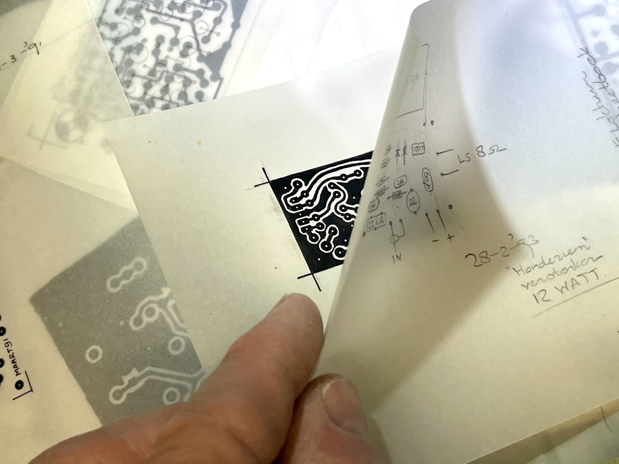
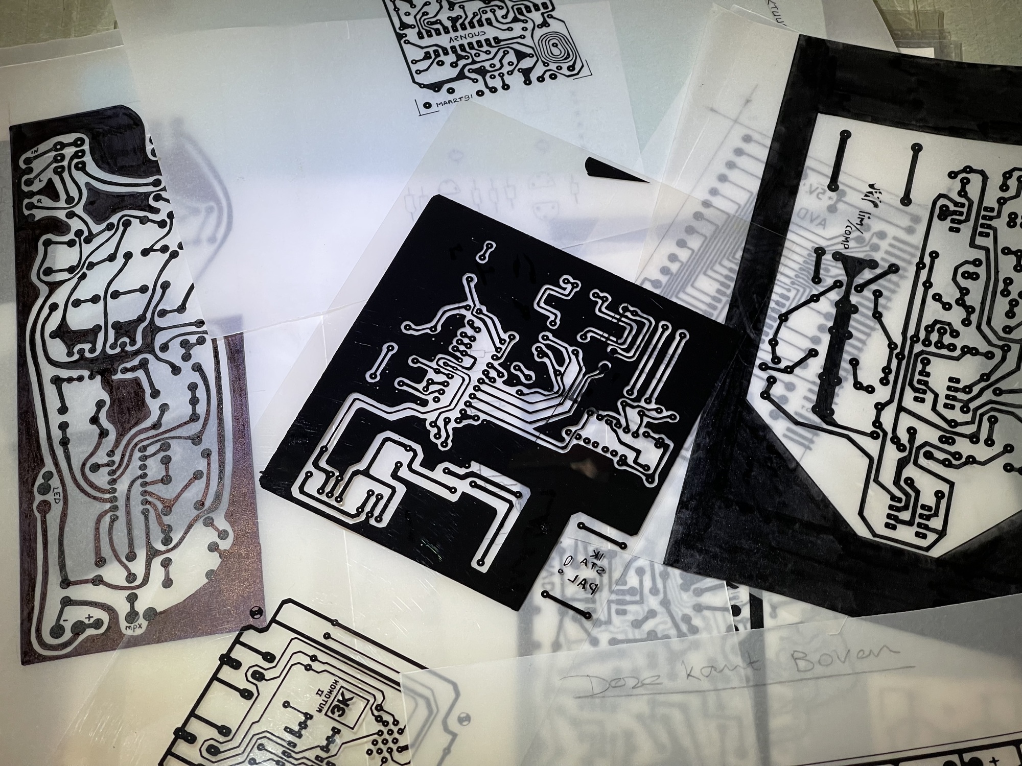
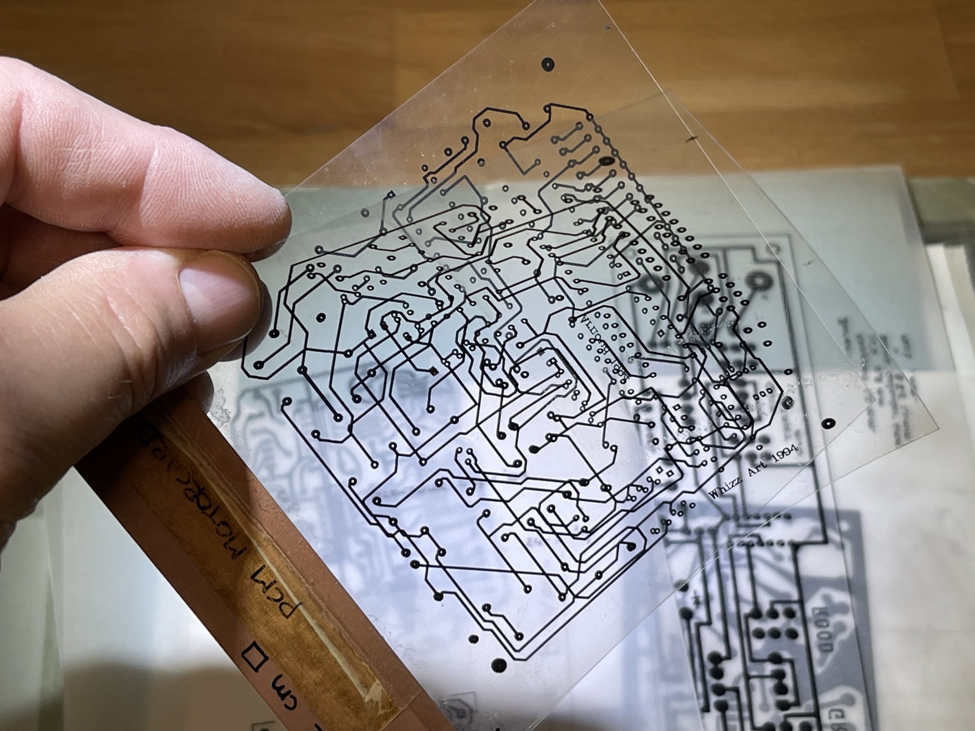
It had been quite some time (almost 35 years) since I made prints myself. Although some designs are still in use, a large container in the attic bears witness to the development trajectory of my creations over the years. In all cases I etched and drilled the PCBs myself. I have tried various methods for transferring the copper traces. With varying degrees of success. In the beginning I drew the entire design, which in those days of course was still simply single-sided, with a waterproof marker on a cleaned piece of print material.
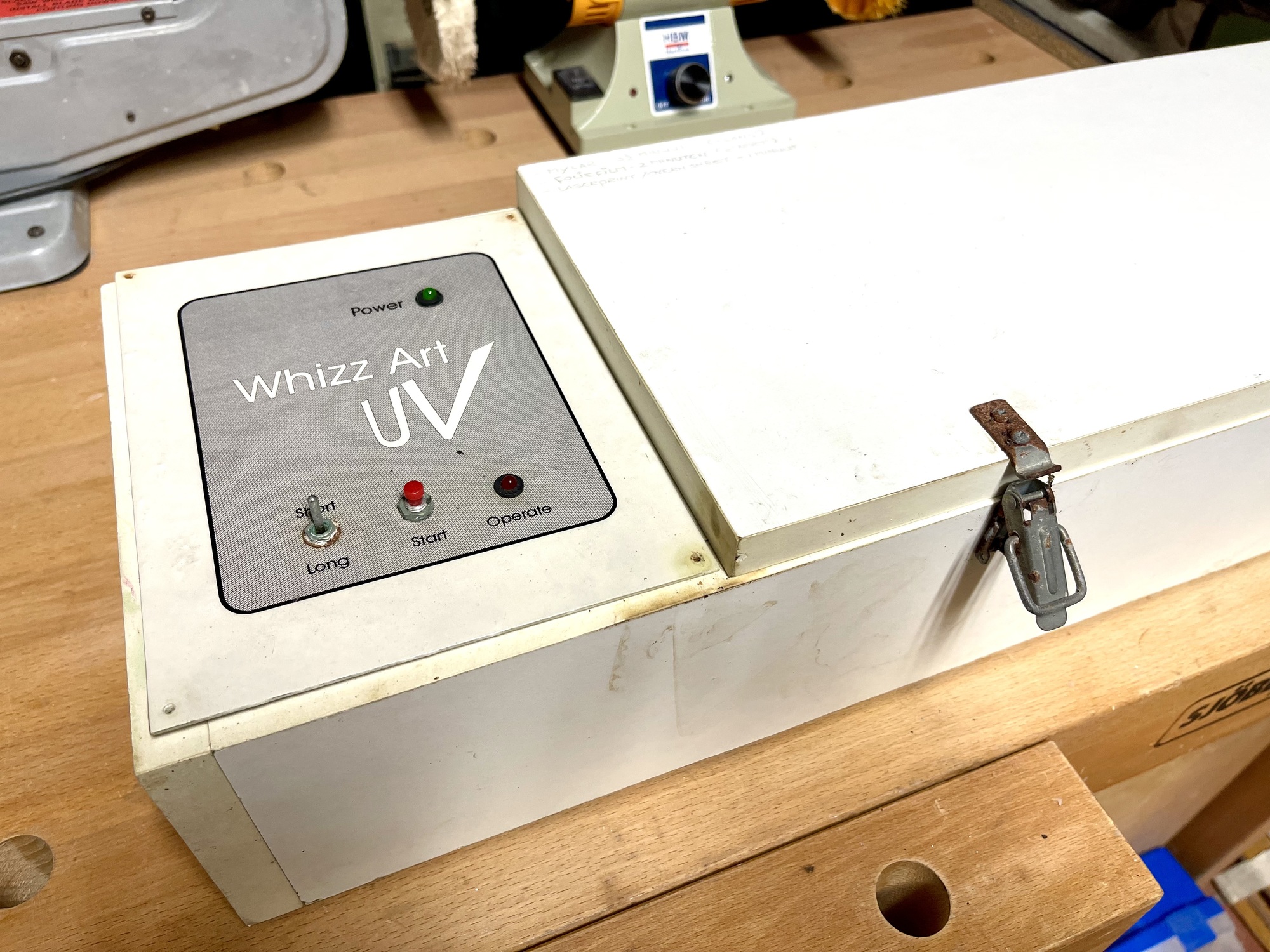
Later I drew the designs by hand on tracing paper, sometimes with the help of rub-off symbols for the copper islands. Or tried, unfortunately not always light-tight, laser-printed overhead sheets. Later still, a real lithograph had it made by a printer friend. With this, photosensitive print material could be exposed on a self-made light box. That listened closely. Too short and the exposed material stuck here and there during the development. Too long and you 'developed' everything away and could also start over.
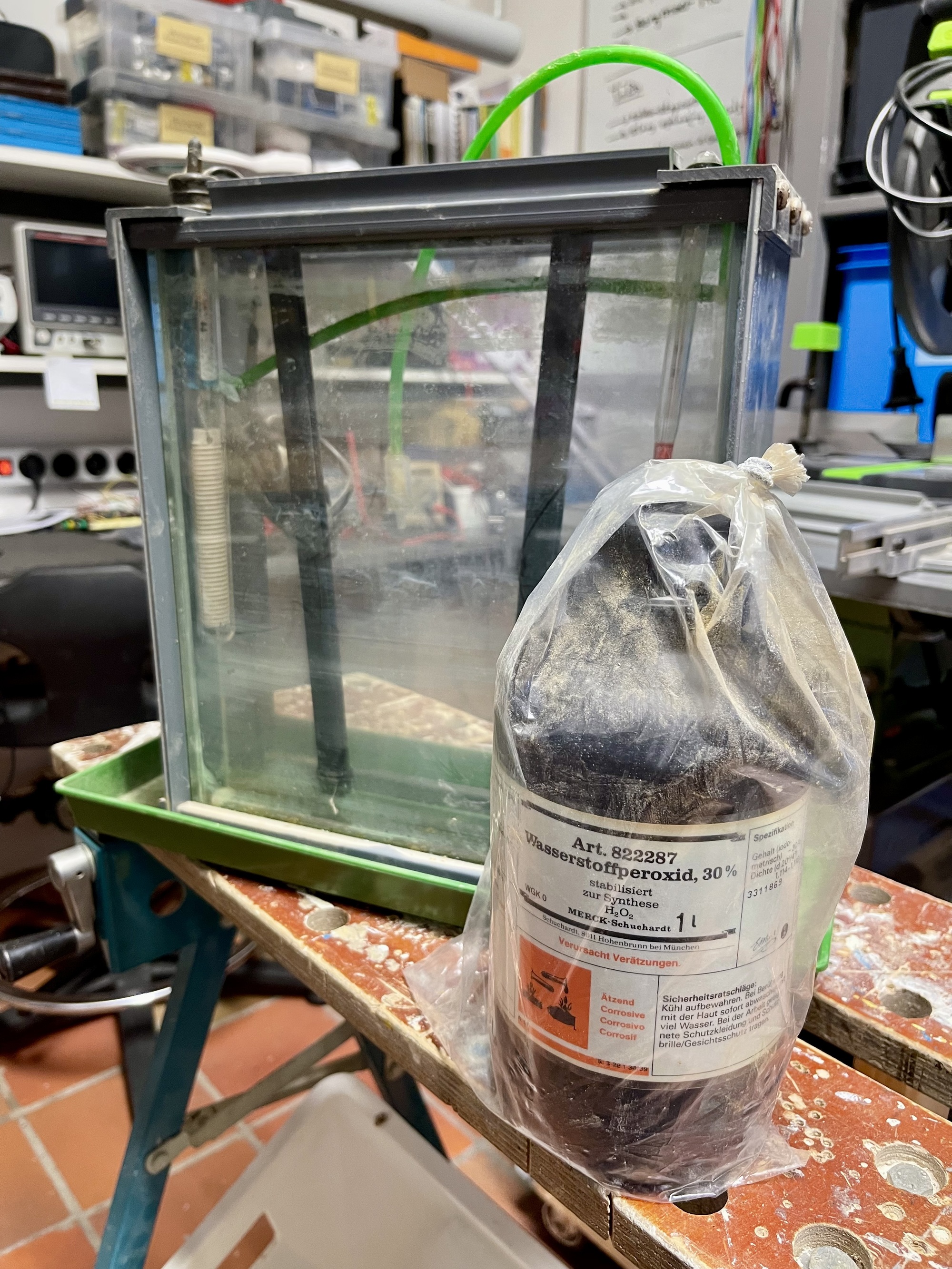
The development was done with a sink plunger and the etching first with the damned yellow iron(III) chloride. That made huge stains and the holes fell into your clothes if you spilled a splash. Later I used a solution of hydrogen peroxide and hydrochloric acid in a heated 'aquarium' that was specially purchased for the etching. It even featured an air fizz pump. This liquid, because it was clear, at least offered a better view of the PCB to determine when it was ready (or simply over-etched again).
Yet, with a lot of fiddling, I have made usable, sometimes even double-sided, prints in this way for years. But also broke a lot of pricey thin printed circuit drills. And of course sometimes just before the last hole was drilled, and the local electronics store was just closed. 😅
With some grits in the shed I was able to find both the light box (from 1993) and the etching bath. Out of piety I took the pictures below because I will soon say goodbye to it. Nice nostalgia, but nowadays having your prints professionally produced is not that expensive anymore and it seemed attractive for this project to go through this process. That way I could update my design skills as well. Previously (in the 1990s) I used a software package called 'Protel' to draw the schematics and design the PCBs. When re-entering, I opted for a solid open-source program that also works great on the Mac: KiCad.
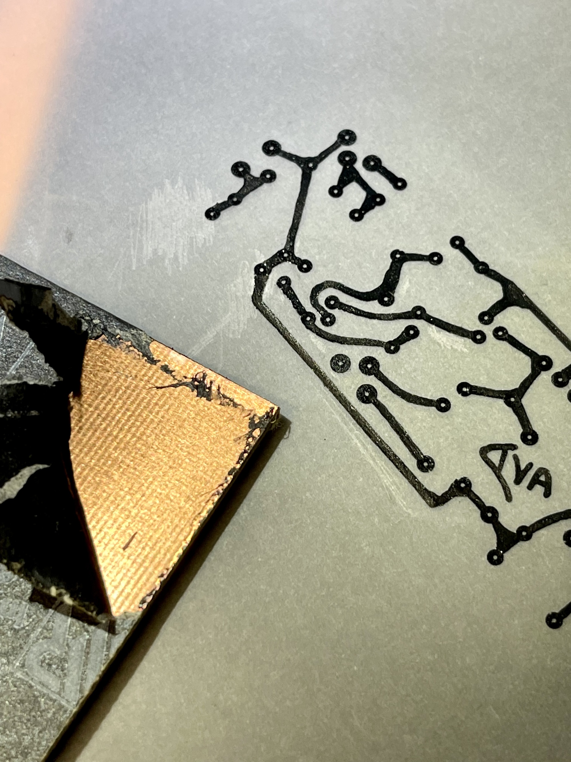
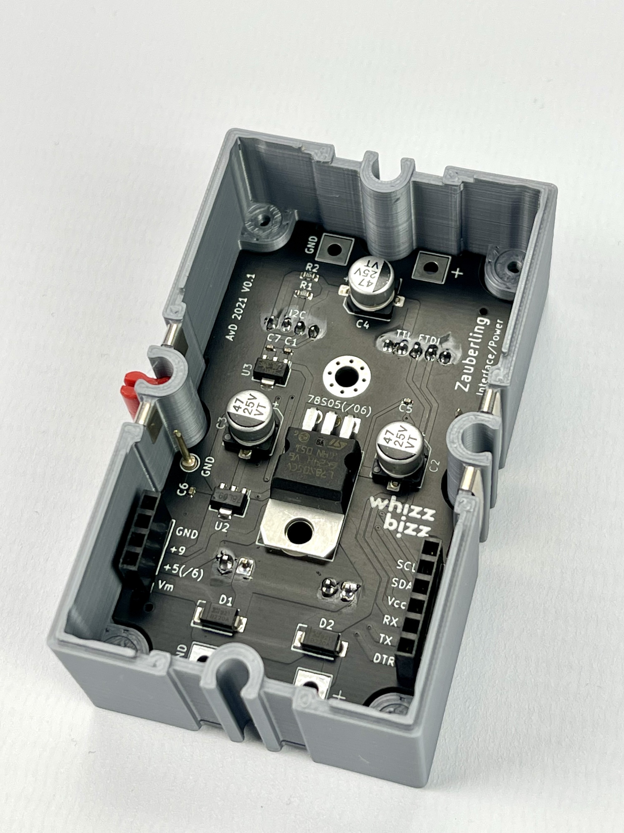
After drawing the schematic and assigning the correct (copper) footprints for all parts, the PCB could be designed. With some experimentation it was possible to get the vector curves from Affinity Designer as 'edge-cut' within KiCad. This will be the actual outline of the PCB, which I had meanwhile made half a millimeter smaller than the inside of the case. I also cut out some space for the support legs inside the case, so that the PCB will fit neatly at the bottom of the cabinet.
Naturally, it is important that the connectors, which must immediately protrude neatly through the recesses at the back, are positioned in the right place on the PCB. The jumper header connectors with the supply voltages, FTDI and I2C bus should be placed at the edge of the PCB as much as possible, so that they do not hinder the placement of parts on the future main PCB of the Zauberling.
Below the result of some shifting and routing of the copper connections. The print is not large, but because you can work on both sides, it is quite easy to connect everything neatly. The 3D representation that KiCad can make immediately gives a good impression of the future end result.


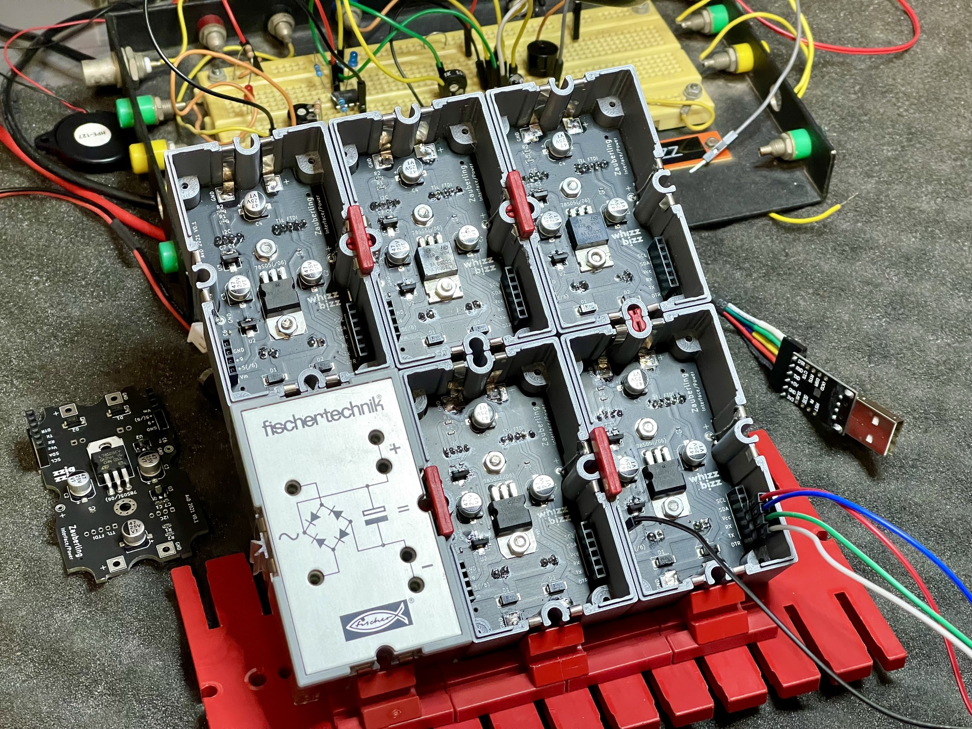
The conclusion cannot be other than that realizing a professional printed circuit board is now a lot easier and cheaper than a few decades ago. It took some figuring out in KiCad, but I soon felt at home in that program. Basically, the development process has remained the same over the years: first draw the well-thought-out scheme and assign the correct footprints to it. Then create the print design. It was also the first time that I used an online printed circuit board producer, but that process also went smoothly. In the photo on the right the PCBs as they arrived almost ready-made, SMD assembled and well.
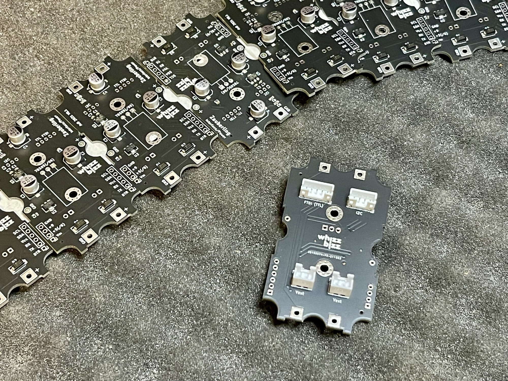
After soldering in the large voltage regulator (depending on the application, a 1, 1.5 or 2 Ampere type), the connection headers and the connectors that protrude through the back, the PCBs were ready to be built in.
The design is of course quite specifically tailored to the (next version of the) Zauberling, but if you want to replicate the power supply PCB, you can find the Gerber files on GitHub. The 3D files for 3D printing the fischertechnik Silberling case are available for everyone to download on Thingiverse.